WSe2 / hBN Field-Effect Transistors
Comparative Analysis of Sample 1 and Sample 2 Characteristics
1. Device Structure & TLM Patterning
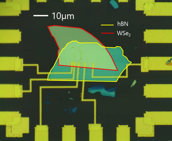
Fig 1a. Sample 1 Optical microscope image showing the WSe2 flake (red outline) transferred onto an hBN flake (yellow outline).
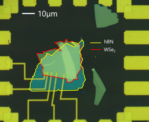
Fig 1b. Sample 2 Optical image of the second fabricated device, maintaining the same heterostructure design.
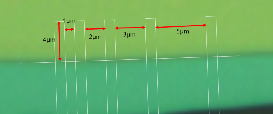
Fig 1c. TLM Pattern The channel lengths are defined as L = 1, 2, 3, and 5 μm, with a uniform channel width of W = 4 μm across all devices.
2. Transfer Characteristics
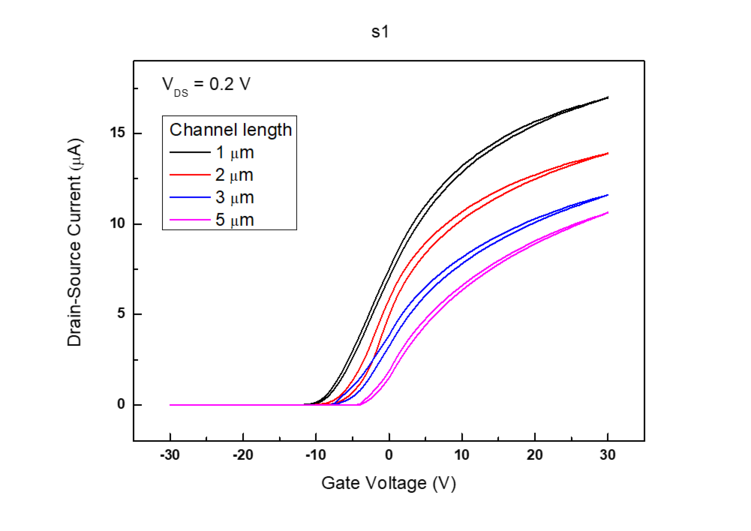
Fig 2a. Sample 1 Transfer Curve (I_D - V_G) measured at V_DS = 0.2V for varying channel lengths.

Fig 2b. Sample 2 Transfer Curve Measured under identical conditions, showing consistent field-effect behavior.
3. Transconductance (g_m)
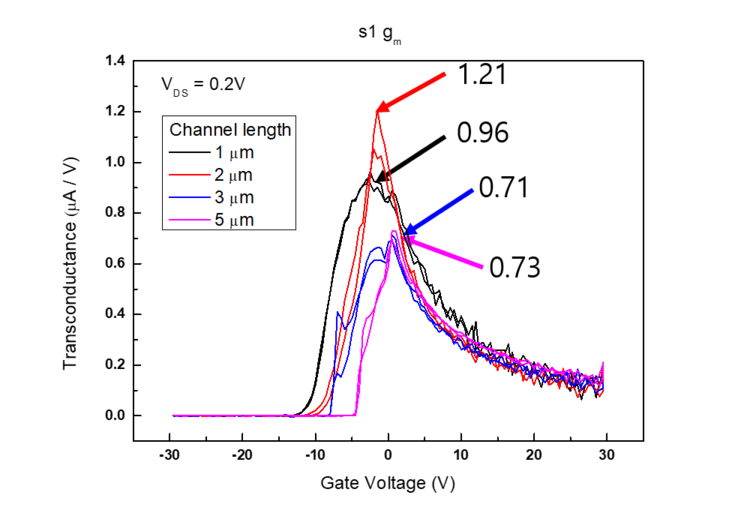
Fig 3a. Sample 1 Transconductance Peak g_m values extracted for each channel length, reaching up to 1.21 μA/V for L = 2 μm.
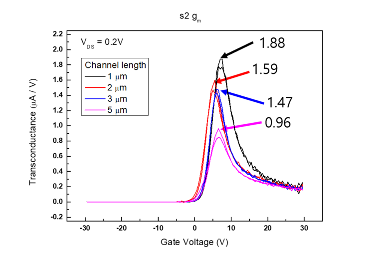
Fig 3b. Sample 2 Transconductance Demonstrating higher peak g_m values compared to Sample 1, with a maximum of 1.88 μA/V for L = 1 μm.
4. Transfer Length Method (TLM) Analysis
To extract the contact resistance (R_c), the total resistance (R_total) is plotted against the channel length (L) using the following relationship:
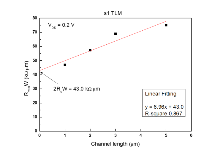
Fig 4a. Sample 1 TLM Fitting Linear fit yields a normalized contact resistance of 2R_c W = 43.0 kΩ·μm with an R-square of 0.867.
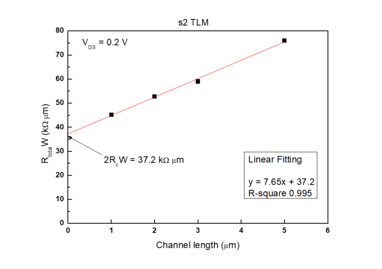
Fig 4b. Sample 2 TLM Fitting Excellent linearity (R-square 0.995) is observed, yielding a lower contact resistance of 2R_c W = 37.2 kΩ·μm.
5. Field-Effect Mobility (\(\mu_{FE}\))
Field-effect mobility is a critical physical quantity representing how easily charge carriers can move within an electric field. The mobility is extracted from the transconductance (\(g_m\)) using the following equation:
where \(L\) and \(W\) are the channel length and width, respectively. \(C_{ox}\) is the area capacitance of the 90 nm SiO\(_2\) dielectric (\(3.84 \times 10^{-4} \text{ F/m}^2\)). By substituting the extracted \(g_m\) and corresponding \(L\) values for each channel, the mobility is calculated as shown in the table below.
| Sample | L [µm] | \(g_m\) [µA/V] | Mobility [cm²/V·s] |
|---|---|---|---|
| #1 | 1 | 0.96 | 31.28 |
| 2 | 1.21 | 78.84 | |
| 3 | 0.71 | 69.39 | |
| 5 | 0.73 | 118.92 | |
| #2 | 1 | 1.88 | 61.25 |
| 2 | 1.59 | 103.60 | |
| 3 | 1.47 | 143.68 | |
| 5 | 0.96 | 156.38 |
Mobility is closely related to defects in the channel region of 2D FET devices and, along with contact resistance, is a crucial factor determining device characteristics. In both samples, we observe a trend where mobility increases as the channel length increases. However, we attribute this result to the fact that in 2D FETs, contact resistance accounts for a relatively larger proportion of the total resistance at shorter channel lengths, leading to an underestimation of the intrinsic mobility in short-channel devices.